• Contact us for Embedded System design, SCADA, IOT, AI, ML Services

Services

Home || PCB Designing

PCB Designing

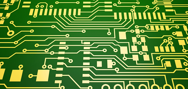
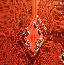
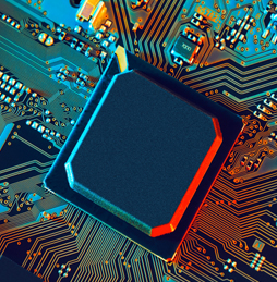
In today's ever-changing digital landscape, there is an increasing demand in the competitive technology market for quality PCB designs. V.S.ELECTRONICS provides you with an ideal selection of design services provided by experts who will assist you in all of your technological requirements while also meeting your demanding schedules.

With the aid of top-tier software and cutting-edge hardware, we specialize in high-performance PCB physical design (layout). Including schematic capture, library development, data base construction and verification, signal integrity, EMI checking, and verification in addition to PCB layout, our skills cover the entire design flow from beginning to end.


Design Capabilities

  •    Schematic and CAD Library Creation and Maintenance
  •    Signal Integrity / Design Verification
  •    High Speed Backplane / Midplane Design
  •    Single Ended and Differential Controlled Impedance Design
  •    Design for Manufacture / Test / Assembly
  •    Micro BGA / Micro Via / Blind & Buried Vias
  •    Full Documentation Package Creation
  •    Handle single-side as well as multi-layer boards
  •    Placement of critical components as per customer specification
  •    Extreme care on critical rout traces as per spec.
  •    For special type of packages footprints can be created.
  •    Manual routing used wherever possible to avoid excess vias and for good aesthetics.
  •    Drill drawing and manufacturing notes can be given as Gerber or a DXF file.